■ 제품필수정보
| 제조사 |
Infineon |
| 제조사품명 |
CY7C1021DV33-10VXI |
| 간략설명 |
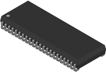
Infineon SRAM Memory Chip, CY7C1021DV33-10VXI- 1Mbit |
■ 제품사양
Memory Size = 1Mbit Organisation = 64k x 16 bit Number of Words = 64k Number of Bits per Word = 16bit Maximum Random Access Time = 10ns Address Bus Width = 16bit Clock Frequency = 1MHz Timing
타입 = Asynchronous
장착형태 = Surface Mount
패키지 = SOJ
핀수 = 44
크기 = 1.13 x 0.405 x 0.12in Maximum Operating Supply Voltage = 3.3 V
최대 작동 온도 = +85 °C This device has an automatic power-down feature that significantly reduces power consumption when deselected. Writing to the device is accomplished by taking Chip Enable (CE) and Write Enable (WE) inputs LOW. If Byte Low Enable (BLE) is LOW, then data from I/O pins (I/O0 through I/O7), is written into the location specified on the address pins (A0 through A15). If Byte High Enable (BHE) is LOW, then data from I/O pins (I/O8 through I/O15) is written into the location specified on the address pins (A0 through A15). Reading from the device is accomplished by taking Chip Enable (CE) and Output Enable (OE) LOW while forcing the Write Enable (WE) HIGH. If Byte Low Enable (BLE) is LOW, then data from the memory location specified by the address pins will appear on I/O0 to I/O7. If Byte High Enable (BHE) is LOW, then data from memory will appear on I/O8 to I/O15. See the truth table at the end of this data sheet for a complete description of Read and Write modes.


