■ 제품필수정보
| 제조사 |
Microchip |
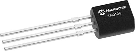
| 제조사품명 |
TN0106N3-G |
| 간략설명 |
N-Channel MOSFET, 350 mA, 60 V, 3-Pin TO-92 Microchip TN0106N3-G |
■ 제품사양
Channel
타입 = N Maximum Continuous Drain Current = 350 mA Maximum Drain Source Voltage = 60 V
패키지 = TO-92
장착형태 = Through Hole
핀수 = 3 Maximum Drain Source Resistance = 4.5 Ω Channel Mode = Enhancement Maximum Gate Threshold Voltage = 2V Minimum Gate Threshold Voltage = 0.6V Maximum Power Dissipation = 1 W Transistor Configuration = Single Maximum Gate Source Voltage = 20 V
최대 작동 온도 = +150 °C Forward Diode Voltage = 1.5V Microchip Technology MOSFETThe Microchip Technology through-hole mount N-channel MOSFET is a new age product with a drain-source resistance of 3ohms at a gate-source voltage of 10V. It has a drain-source voltage of 60V and a maximum gate-source voltage of 20V. It has continuous drain current of 350mA and maximum power dissipation of 1W. The minimum and a maximum driving voltage for this MOSFET is 4.5V and 10V respectively. The MOSFET is an enhancement mode (normally off) transistor that utilizes a vertical DMOS structure and well-proven, silicon gate manufacturing process. This combination produces a device with the power handling capabilities of bipolar transistors and the high input impedance and positive temperature coefficient inherent in MOS devices. A significant characteristic of all MOS structures, this device is free from thermal runaway and thermally induced secondary breakdown. This vertical DMOS FET has been optimized for lower switching and conduction losses. The MOSFET offers excellent efficiency along with a long and productive life without compromising performance or functionality.Features and Benefits??Ease of paralleling ??Excellent thermal stability ??Free from secondary breakdown ??High input impedance and high gain ??Integral source drain diode ??Low CISS and fast switching speeds ??Low power drive requirement ??Operating temperature ranges between -55°C and 150°CApplications??Analog switches ??Battery operated systems ??General purpose line drivers ??Logic level interfaces - ideal for TTL and CMOS ??Photo voltaic drives ??Solid state relays ??Telecom switchesCertifications??ANSI/ESD S20.20:2014 ??BS EN 61340-5-1:2007 ??JEDEC